

What Does Pc4 Mean On Ram
| Type of RAM | |
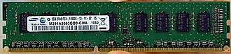
 16 GiB[1] DDR4-2666 1.2 V UDIMM | |
| Programmer | JEDEC |
|---|---|
| Type | Synchronous dynamic random-access memory (SDRAM) |
| Generation | 4th generation |
| Release date | 2014 (2014) |
| Standards |
|
| Clock rate | 800–1600 MHz |
| Voltage | Reference 1.2 Five |
| Predecessor | DDR3 SDRAM (2007) |
| Successor | DDR5 SDRAM (2020) |
Double Data Rate 4 Synchronous Dynamic Random-Access Memory (DDR4 SDRAM) is a type of synchronous dynamic random-access memory with a high bandwidth ("double data rate") interface.
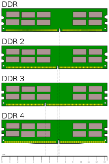
Released to the market in 2014,[two] [3] [four] it is a variant of dynamic random-access memory (DRAM), of which some have been in employ since the early 1970s,[5] and a higher-speed successor to the DDR2 and DDR3 technologies.
DDR4 is not uniform with whatever earlier type of random-admission retentiveness (RAM) due to dissimilar signaling voltage and physical interface, besides other factors.
DDR4 SDRAM was released to the public marketplace in Q2 2014, focusing on ECC memory,[vi] while the not-ECC DDR4 modules became available in Q3 2014, accompanying the launch of Haswell-East processors that require DDR4 memory.[7]
Features [edit]
The principal advantages of DDR4 over its predecessor, DDR3, include higher module density and lower voltage requirements, coupled with higher data rate transfer speeds. The DDR4 standard allows for DIMMs of up to 64 GB in capacity, compared to DDR3's maximum of 16 GB per DIMM.[1] [8] [ failed verification ]
Unlike previous generations of DDR retentivity, prefetch has not been increased in a higher place the 8n used in DDR3;[nine] : sixteen the basic burst size is eight 64-bit words, and college bandwidths are achieved by sending more read/write commands per 2d. To allow this, the standard divides the DRAM banks into ii or 4 selectable bank groups,[ten] where transfers to different bank groups may be done more rapidly.
Because power consumption increases with speed, the reduced voltage allows higher speed functioning without unreasonable power and cooling requirements.
DDR4 operates at a voltage of one.two 5 with a frequency between 800 and 1600 MHz (DDR4-1600 through DDR4-3200), compared to frequencies between 400 and 1067 MHz (DDR3-800 through DDR3-2133)[11] [a] and voltage requirements of 1.5 V of DDR3. Due to the nature of DDR, speeds are typically advertised every bit doubles of these numbers (DDR3-1600 and DDR4-2400 are common, with DDR4-3200, DDR4-4800 and DDR4-5000 bachelor at loftier cost). Dissimilar DDR3'south 1.35 Five depression voltage standard DDR3L, there is no DDR4L depression voltage version of DDR4.[13] [xiv]
Timeline [edit]
The first DDR4 retentiveness module prototype was manufactured by Samsung and announced in January 2011.[b]
Forepart and back of viii GB[ane] DDR4 retention modules
- 2005: Standards torso JEDEC began working on a successor to DDR3 around 2005,[16] about ii years before the launch of DDR3 in 2007.[17] [xviii] The high-level architecture of DDR4 was planned for completion in 2008.[19]
- 2007: Some accelerate information was published in 2007,[20] and a guest speaker from Qimonda provided further public details in a presentation at the August 2008 San Francisco Intel Programmer Forum (IDF).[20] [21] [22] [23] DDR4 was described as involving a 30 nm process at 1.ii volts, with autobus frequencies of 2133 MT/due south "regular" speed and 3200 MT/s "enthusiast" speed, and reaching market in 2012, earlier transitioning to 1 volt in 2013.[21] [23]
- 2009: In February, Samsung validated 40 nm DRAM chips, considered a "significant footstep" towards DDR4 evolution[24] since in 2009, DRAM fries were only beginning to drift to a 50 nm process.[25]
- 2010: Subsequently, further details were revealed at MemCon 2010, Tokyo (a computer memory industry outcome), at which a presentation by a JEDEC director titled "Time to rethink DDR4"[26] with a slide titled "New roadmap: More realistic roadmap is 2015" led some websites to report that the introduction of DDR4 was probably[27] or definitely[28] [29] delayed until 2015. However, DDR4 test samples were appear in line with the original schedule in early 2011 at which time manufacturers began to suggest that large scale commercial production and release to market was scheduled for 2012.[2]
- 2011: In January, Samsung announced the completion and release for testing of a two GB[1] DDR4 DRAM module based on a process betwixt xxx and 39 nm.[thirty] It has a maximum data transfer rate of 2133 MT/s at i.2 Five, uses pseudo open bleed applied science (adapted from graphics DDR memory[31]) and draws 40% less ability than an equivalent DDR3 module.[30] [32] [33]
In April, Hynix announced the product of two GB[one] DDR4 modules at 2400 MT/s, likewise running at 1.2 Five on a process between thirty and 39 nm (exact process unspecified),[2] calculation that information technology anticipated commencing high volume production in the second half of 2012.[2] Semiconductor processes for DDR4 are expected to transition to sub-thirty nm at some point between late 2012 and 2014.[34] [35] [ needs update ] - 2012: In May, Micron announced[3] it is aiming at starting production in late 2012 of 30 nm modules.
In July, Samsung announced that it would begin sampling the industry'south offset xvi GB[ane] registered dual inline retentiveness modules (RDIMMs) using DDR4 SDRAM for enterprise server systems.[36] [37]
In September, JEDEC released the final specification of DDR4.[38] - 2013: DDR4 was expected to correspond 5% of the DRAM market place in 2013,[ii] and to reach mass market adoption and 50% market penetration around 2015;[ii] as of 2013, however, adoption of DDR4 had been delayed and it was no longer expected to attain a majority of the marketplace until 2016 or later.[39] The transition from DDR3 to DDR4 is thus taking longer than the approximately 5 years taken for DDR3 to achieve mass marketplace transition over DDR2.[34] In office, this is because changes required to other components would touch on all other parts of figurer systems, which would need to exist updated to work with DDR4.[40]
- 2014: In April, Hynix appear that it had developed the world's get-go highest-density 128 GB module based on viii Gbit DDR4 using 20 nm technology. The module works at 2133 MHz, with a 64-bit I/O, and processes up to 17 GB of information per 2d.
- 2016: In April, Samsung announced that they had begun to mass-produce DRAM on a "x nm-grade" procedure, by which they mean the 1x nm node regime of sixteen nm to xix nm, which supports a xxx% faster data transfer rate of three,200 Mbit/s.[41] Previously, a size of 20 nm was used.[42] [43]
Market place perception and adoption [edit]
In April 2013, a news writer at International Data Group (IDG) – an American engineering inquiry business organisation originally part of IDC – produced an analysis of their perceptions related to DDR4 SDRAM.[44] The conclusions were that the increasing popularity of mobile computing and other devices using slower but depression-powered memory, the slowing of growth in the traditional desktop computing sector, and the consolidation of the memory manufacturing market place, meant that margins on RAM were tight.
Every bit a result, the desired premium pricing for the new technology was harder to achieve, and capacity had shifted to other sectors. SDRAM manufacturers and chipset creators were, to an extent, "stuck between a stone and a hard place" where "nobody wants to pay a premium for DDR4 products, and manufacturers don't want to brand the retention if they are non going to become a premium", co-ordinate to Mike Howard from iSuppli.[44] A switch in consumer sentiment toward desktop computing and release of processors having DDR4 support by Intel and AMD could therefore potentially lead to "aggressive" growth.[44]
Intel'southward 2014 Haswell roadmap, revealed the company's first use of DDR4 SDRAM in Haswell-EP processors.[45]
AMD'due south Ryzen processors, revealed in 2016 and shipped in 2017, use DDR4 SDRAM.[46]
Operation [edit]
| | This department needs to be updated. (Jan 2014) |
DDR4 chips use a 1.ii V supply[9] : 16 [47] [48] with a 2.v V auxiliary supply for wordline boost chosen VPP,[ix] : 16 equally compared with the standard one.5 Five of DDR3 chips, with lower voltage variants at 1.35 5 appearing in 2013. DDR4 is expected to be introduced at transfer rates of 2133 MT/s,[ix] : 18 estimated to ascent to a potential 4266 MT/s[twoscore] by 2013. The minimum transfer rate of 2133 MT/south was said to be due to progress made in DDR3 speeds which, existence likely to accomplish 2133 MT/southward, left niggling commercial benefit to specifying DDR4 below this speed.[34] [40] Techgage interpreted Samsung'due south January 2011 technology sample every bit having CAS latency of 13 clock cycles, described as existence comparable to the motion from DDR2 to DDR3.[31]
Internal banks are increased to sixteen (4 bank select bits), with up to 8 ranks per DIMM.[ix] : 16
Protocol changes include:[9] : 20
- Parity on the control/address bus
- Data bus inversion (like GDDR4)
- CRC on the information coach
- Independent programming of private DRAMs on a DIMM, to permit better command of on-die termination.
Increased retentivity density is anticipated, possibly using TSV ("through-silicon via") or other 3D stacking processes.[34] [40] [49] [50] The DDR4 specification will include standardized 3D stacking "from the start" according to JEDEC,[50] with provision for up to eight stacked dies.[nine] : 12 Ten-bit Labs predicted that "as a result DDR4 retentiveness fries with very high density volition become relatively inexpensive".[40]
Switched memory banks are also an anticipated option for servers.[34] [49]
In 2008 concerns were raised in the volume Wafer Level iii-D ICs Process Technology that not-scaling analog elements such as charge pumps and voltage regulators, and additional circuitry "accept allowed significant increases in bandwidth merely they consume much more than die area". Examples include CRC fault-detection, on-die termination, burst hardware, programmable pipelines, low impedance, and increasing need for sense amps (attributed to a refuse in $.25 per bitline due to low voltage). The authors noted that, equally a result, the amount of dice used for the retention array itself has declined over time from seventy–78% for SDRAM and DDR1, to 47% for DDR2, to 38% for DDR3 and to potentially less than 30% for DDR4.[51]
The specification defined standards for ×four, ×eight and ×16 retention devices with capacities of 2, 4, viii and 16 GB.[1] [52]
In addition to bandwidth and capacity variants, DDR4 modules can optionally implement:
- ECC, which is an actress information byte lane used for correcting minor errors and detecting major errors for improve reliability. Modules with ECC are identified past an additional ECC in their designation. PC4-19200 ECC or PC4-19200E is a PC4-19200 module with ECC.[53]
- Exist "registered" ("buffered"), which improves signal integrity (and hence potentially clock rates and physical slot capacity) by electrically buffering the signals at a cost of an actress clock of increased latency. Those modules are identified by an boosted R in their designation, e.one thousand. PC4-19200R. Typically modules with this designation are actually ECC Registered, but the 'East' of 'ECC' is not always shown. Whereas non-registered (a.k.a. unbuffered RAM) may be identified by an additional U in the designation. e.g. PC4-19200U.[53]
- Be Load reduced modules, which are designated past LR and are similar to registered/buffered retention, in a mode that LRDIMM modules buffer both control and data lines while retaining the parallel nature of all signals. Equally such, LRDIMM memory provides larger overall maximum retention capacities, while addressing some of the performance and ability consumption issues of FB retention induced by the required conversion between serial and parallel point forms.[53]
Command encoding [edit]
Although it still operates in fundamentally the same way, DDR4 makes one major alter to the command formats used by previous SDRAM generations. A new command signal, ACT, is depression to betoken the activate (open row) command.
The activate command requires more address bits than any other (18 row address bits in a 16 Gbit part), so the standard RAS, CAS, and Nosotros active low signals are shared with high-order address $.25 that are not used when Act is high. The combination of RAS=L and CAS=We=H that previously encoded an activate command is unused.
As in previous SDRAM encodings, A10 is used to select command variants: machine-precharge on read and write commands, and one banking company vs. all banks for the precharge command. It also selects two variants of the ZQ scale control.
As in DDR3, A12 is used to asking burst chop: truncation of an eight-transfer outburst after 4 transfers. Although the bank is withal busy and unavailable for other commands until eight transfer times accept elapsed, a dissimilar banking concern can exist accessed.
Besides, the number of banking company addresses has been increased greatly. In that location are iv bank select bits to select up to 16 banks within each DRAM: 2 depository financial institution address bits (BA0, BA1), and two bank group bits (BG0, BG1). There are additional timing restrictions when accessing banks within the same bank group; it is faster to access a banking company in a different bank group.
In addition, in that location are three scrap select signals (C0, C1, C2), allowing upwards to eight stacked fries to be placed inside a single DRAM packet. These effectively human activity as three more than banking company select $.25, bringing the total to vii (128 possible banks).
Standard transfer rates are 1600, 1866, 2133, 2400, 2666, 2933, and 3200 MT/s[54] [55] ( 12⁄15 , 14⁄15 , 16⁄fifteen , 18⁄fifteen , 20⁄15 , 22⁄15 , and 24⁄15 GHz clock frequencies, double information rate), with speeds upwardly to DDR4-4800 (2400 MHz clock) commercially bachelor.[56]
Blueprint considerations [edit]
The DDR4 team at Micron Technology identified some key points for IC and PCB design:[57]
IC design:[57]
- VrefDQ scale (DDR4 "requires that VrefDQ calibration be performed by the controller");
- New addressing schemes ("banking concern grouping", Human activity to supervene upon RAS, CAS, and WE commands, PAR and Warning for mistake checking and DBI for data bus inversion);
- New power saving features (low-power auto self-refresh, temperature-controlled refresh, fine-granularity refresh, data-bus inversion, and CMD/ADDR latency).
Circuit board blueprint:[57]
- New power supplies (VDD/VDDQ at 1.2 V and wordline boost, known as VPP, at 2.5 V);
- VrefDQ must be supplied internal to the DRAM while VrefCA is supplied externally from the board;
- DQ pins end high using pseudo-open-drain I/O (this differs from the CA pins in DDR3 which are center-tapped to VTT).[57]
Rowhammer mitigation techniques include larger storage capacitors, modifying the address lines to use address space layout randomization and dual-voltage I/O lines that further isolate potential purlieus conditions that might result in instability at high write/read speeds.
Module packaging [edit]
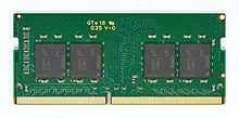
A 16GB[ane] DDR4 And so-DIMM module by Micron
DDR4 retentiveness is supplied in 288-pin dual in-line retentiveness modules (DIMMs), similar in size to 240-pin DDR3 DIMMs. The pins are spaced more closely (0.85 mm instead of 1.0) to fit the increased number within the same 5¼ inch (133.35 mm) standard DIMM length, merely the summit is increased slightly (31.25 mm/1.23 in instead of 30.35 mm/ane.2 in) to make signal routing easier, and the thickness is too increased (to 1.2 mm from i.0) to accommodate more signal layers.[58] DDR4 DIMM modules take a slightly curved edge connector so not all of the pins are engaged at the same time during module insertion, lowering the insertion force.[15]
DDR4 SO-DIMMs have 260 pins instead of the 204 pins of DDR3 Then-DIMMs, spaced at 0.five rather than 0.half-dozen mm, and are 2.0 mm wider (69.6 versus 67.6 mm), only remain the aforementioned thirty mm in height.[59]
For its Skylake microarchitecture, Intel designed a SO-DIMM bundle named UniDIMM, which tin be populated with either DDR3 or DDR4 chips. At the same fourth dimension, the integrated retentivity controller (IMC) of Skylake CPUs is announced to be capable of working with either type of memory. The purpose of UniDIMMs is to help in the market transition from DDR3 to DDR4, where pricing and availability may get in undesirable to switch the RAM blazon. UniDIMMs have the same dimensions and number of pins as regular DDR4 SO-DIMMs, just the edge connector'due south notch is placed differently to avert accidental use in incompatible DDR4 SO-DIMM sockets.[sixty]
Modules [edit]
JEDEC standard DDR4 module [edit]
| Standard name | Memory clock (MHz) | I/O bus clock (MHz) | Data rate (MT/s)[c] | Module name | Summit trans- fer rate (MB/southward)[d] | Timings CL-tRCD-tRP | CAS latency (ns) |
|---|---|---|---|---|---|---|---|
| DDR4-1600J* DDR4-1600K DDR4-1600L | 200 | 800 | 1600 | PC4-12800 | 12800 | 10-ten-x eleven-eleven-11 12-12-12 | 12.five 13.75 15 |
| DDR4-1866L* DDR4-1866M DDR4-1866N | 233.33 | 933.33 | 1866.67 | PC4-14900 | 14933.33 | 12-12-12 13-13-xiii 14-fourteen-xiv | 12.857 xiii.929 15 |
| DDR4-2133N* DDR4-2133P DDR4-2133R | 266.67 | 1066.67 | 2133.33 | PC4-17000 | 17066.67 | 14-14-14 15-fifteen-15 16-sixteen-16 | 13.125 14.063 xv |
| DDR4-2400P* DDR4-2400R DDR4-2400T DDR4-2400U | 300 | 1200 | 2400 | PC4-19200 | 19200 | xv-15-xv 16-16-16 17-17-17 xviii-xviii-eighteen | 12.5 13.32 fourteen.16 fifteen |
| DDR4-2666T DDR4-2666U DDR4-2666V DDR4-2666W | 333.33 | 1333.33 | 2666.67 | PC4-21300 | 21333.33 | 17-17-17 eighteen-xviii-18 19-xix-19 20-xx-20 | 12.75 13.50 xiv.25 fifteen |
| DDR4-2933V DDR4-2933W DDR4-2933Y DDR4-2933AA | 366.67 | 1466.67 | 2933.33 | PC4-23466 | 23466.67 | 19-19-xix 20-20-twenty 21-21-21 22-22-22 | 12.96 xiii.64 xiv.32 15 |
| DDR4-3200W DDR4-3200AA DDR4-3200AC | 400 | 1600 | 3200 | PC4-25600 | 25600 | 20-20-20 22-22-22 24-24-24 | 12.5 13.75 15 |
- CAS latency (CL)
- Clock cycles betwixt sending a cavalcade accost to the memory and the first of the data in response
- tRCD
- Clock cycles between row actuate and reads/writes
- tRP
- Clock cycles between row precharge and activate
DDR4-xxxx denotes per-bit data transfer rate, and is normally used to describe DDR chips. PC4-xxxxx denotes overall transfer rate, in megabytes per 2d, and applies merely to modules (assembled DIMMs). Because DDR4 memory modules transfer data on a bus that is 8 bytes (64 data bits) wide, module peak transfer rate is calculated by taking transfers per second and multiplying past 8.[61]
Successor [edit]
At the 2016 Intel Developer Forum, the future of DDR5 SDRAM was discussed. The specifications were finalized at the end of 2016 – only no modules volition be available before 2020.[62] Other retention technologies – namely HBM in version 3 and 4[63] – aiming to replace DDR4 have also been proposed.
In 2011, JEDEC published the Wide I/O 2 standard; information technology stacks multiple memory dies, just does that straight on top of the CPU and in the same packet. This memory layout provides college bandwidth and better power performance than DDR4 SDRAM, and allows a wide interface with short signal lengths. It primarily aims to supervene upon various mobile DDRX SDRAM standards used in high-functioning embedded and mobile devices, such as smartphones.[64] [65] Hynix proposed similar High Bandwidth Memory (HBM), which was published as JEDEC JESD235. Both Wide I/O two and HBM use a very broad parallel memory interface, up to 512 bits wide for Broad I/O 2 (compared to 64 $.25 for DDR4), running at a lower frequency than DDR4.[66] Wide I/O 2 is targeted at loftier-performance meaty devices such as smartphones, where information technology will be integrated into the processor or organization on a scrap (SoC) packages. HBM is targeted at graphics memory and general computing, while HMC targets loftier-cease servers and enterprise applications.[66]
Micron Technology'southward Hybrid Retentiveness Cube (HMC) stacked memory uses a serial interface. Many other calculator buses have migrated towards replacing parallel buses with serial buses, for case by the development of Serial ATA replacing Parallel ATA, PCI Express replacing PCI, and serial ports replacing parallel ports. In general, serial buses are easier to calibration up and accept fewer wires/traces, making excursion boards using them easier to design.[67] [68] [69]
In the longer term, experts speculate that not-volatile RAM types like PCM (phase-alter memory), RRAM (resistive random-access retentiveness), or MRAM (magnetoresistive random-access retention) could replace DDR4 SDRAM and its successors.[70]
GDDR5 SGRAM is a graphics type of DDR3 synchronous graphics RAM, which was introduced earlier DDR4, and is not a successor to DDR4.
See as well [edit]
- Synchronous dynamic random access memory – master article for DDR memory types
- Listing of device bandwidths
- Memory timings
Notes [edit]
- ^ Some manufactory-overclocked DDR3 memory modules operate at college frequencies, upward to 1600 MHz.[12] [ failed verification ]
- ^ As a epitome, this DDR4 retentiveness module has a flat edge connector at the lesser, while product DDR4 DIMM modules have a slightly curved edge connector and then not all of the pins are engaged at a fourth dimension during module insertion, lowering the insertion strength.[xv]
- ^ 1 MT = one one thousand thousand transfers
- ^ 1 MB = one million bytes
References [edit]
- ^ a b c d e f g h Hither, Chiliad, M, Thousand, or T refer to the binary prefixes based on powers of 1024.
- ^ a b c d e f Marc (2011-04-05). "Hynix produces its first DDR4 modules". Exist hardware. Archived from the original on 2012-04-fifteen. Retrieved 2012-04-14 .
- ^ a b Micron teases working DDR4 RAM, Engadget, 2012-05-08, retrieved 2012-05-08
- ^ "Samsung mass-produces DDR4". Retrieved 2013-08-31 .
- ^ The DRAM Story (PDF), IEEE, 2008, p. x, retrieved 2012-01-23
- ^ "Crucial DDR4 Server Retentiveness Now Available". Earth newswire. 2 June 2014. Retrieved 12 December 2014.
- ^ btarunr (14 September 2014). "How Intel Plans to Transition Between DDR3 and DDR4 for the Mainstream". TechPowerUp . Retrieved 28 April 2015.
- ^ Wang, David (12 March 2013). "Why migrate to DDR4?". Inphi Corp. – via EE Times.
- ^ a b c d e f thousand Jung, JY (2012-09-xi), "How DRAM Advancements are Impacting Server Infrastructure", Intel Developer Forum 2012, Intel, Samsung; Active events, archived from the original on 2012-11-27, retrieved 2012-09-15
- ^ "Master Memory: DDR4 & DDR5 SDRAM". JEDEC. Retrieved 2012-04-14 .
- ^ "DDR3 SDRAM Standard JESD79-3F, sec. Table 69 – Timing Parameters by Speed Bin". JEDEC. July 2012. Retrieved 2015-07-eighteen .
- ^ "Vengeance LP Memory — 8GB 1600MHz CL9 DDR3 (CML8GX3M1A1600C9)". Corsair . Retrieved 17 July 2015.
- ^ "DDR4 – Advantages of Migrating from DDR3", Products , retrieved 2014-08-20 .
- ^ "Corsair unleashes world's fastest DDR4 RAM and 16GB costs more than than your gaming PC (probably) | TechRadar". world wide web.techradar.com.
- ^ a b "Molex DDR4 DIMM Sockets, Halogen-gratuitous". Arrow Europe. Molex. 2012. Retrieved 2015-06-22 .
- ^ Sobolev, Vyacheslav (2005-05-31). "JEDEC: Retention standards on the way". Digitimes. Via tech. Archived from the original on 2013-12-03. Retrieved 2011-04-28 .
Initial investigations have already started on memory technology beyond DDR3. JEDEC always has most three generations of memory in various stages of the standardization procedure: current generation, next generation, and future.
- ^ "DDR3: Frequently asked questions" (PDF). Kingston Engineering science. Archived from the original (PDF) on 2011-07-28. Retrieved 2011-04-28 .
DDR3 retentiveness launched in June 2007
- ^ Valich, Theo (2007-05-02). "DDR3 launch gear up for May 9th". The Inquirer. Archived from the original on Feb 5, 2010. Retrieved 2011-04-28 .
{{cite news}}: CS1 maint: unfit URL (link) - ^ Hammerschmidt, Christoph (2007-08-29). "Non-volatile memory is the secret star at JEDEC meeting". EE Times . Retrieved 2011-04-28 .
- ^ a b "DDR4 – the successor to DDR3 memory". The "H" (online ed.). 2008-08-21. Archived from the original on 26 May 2011. Retrieved 2011-04-28 .
The JEDEC standardisation committee cited similar figures around i twelvemonth ago
- ^ a b Graham-Smith, Darien (2008-08-19). "IDF: DDR3 won't catch up with DDR2 during 2009". PC Pro. Archived from the original on 2011-06-07. Retrieved 2011-04-28 .
- ^ Volker, Rißka (2008-08-21). "IDF: DDR4 als Hauptspeicher ab 2012" [Intel Developer Forum: DDR4 as the principal memory from 2012]. Computerbase (in German language). DE. Retrieved 2011-04-28 . (English)
- ^ a b Novakovic, Nebojsa (2008-08-nineteen). "Qimonda: DDR3 moving frontward". The Inquirer. Archived from the original on Nov 25, 2010. Retrieved 2011-04-28 .
{{cite web}}: CS1 maint: unfit URL (link) - ^ Gruener, Wolfgang (February 4, 2009). "Samsung hints to DDR4 with get-go validated 40 nm DRAM". TG daily. Archived from the original on May 24, 2009. Retrieved 2009-06-16 .
- ^ Jansen, Ng (Jan 20, 2009). "DDR3 Will be Cheaper, Faster in 2009". Dailytech. Archived from the original on June 22, 2009. Retrieved 2009-06-17 .
- ^ Gervasi, Beak. "Fourth dimension to rethink DDR4" (PDF). July 2010. Discobolus Designs. Retrieved 2011-04-29 .
- ^ "DDR4-Speicher kommt wohl später als bisher geplant" [DDR4 memory is probably later than previously planned]. Heise (in German). DE. 2010-08-17. Retrieved 2011-04-29 . (English)
- ^ Nilsson, Lars-Göran (2010-08-16). "DDR4 not expected until 2015". Semi accurate . Retrieved 2011-04-29 .
- ^ annihilator (2010-08-18). "DDR4 retentiveness in Works, Volition attain 4.266 GHz". WCCF tech . Retrieved 2011-04-29 .
- ^ a b "Samsung Develops Manufacture's Starting time DDR4 DRAM, Using 30nm Class Technology". Samsung. 2011-04-11. Retrieved 26 Apr 2011.
- ^ a b Perry, Ryan (2011-01-06). "Samsung Develops the First 30nm DDR4 DRAM". Tech gage . Retrieved 2011-04-29 .
- ^ "Samsung Develops Industry's First DDR4 DRAM, Using 30 nm Class Applied science" (press release). Samsung. 2011-01-04. Retrieved 2011-03-13 .
- ^ Protalinski, Emil (2011-01-04), Samsung develops DDR4 memory, upwards to forty% more than efficient, Techspot, retrieved 2012-01-23
- ^ a b c d e 後藤, 弘茂 [Gotou Shigehiro]. "メモリ4Gbps時代へと向かう次世代メモリDDR4" [Towards Next-Generation 4Gbps DDR4 Memory]. 2010-08-16 (in Japanese). JP: PC Scout. Retrieved 2011-04-25 . (English language translation)
- ^ "Diagram: Predictable DDR4 timeline". 2010-08-sixteen. JP: PC Watch. Retrieved 2011-04-25 .
- ^ "Samsung Samples Industry's First DDR4 Memory Modules for Servers" (printing release). Samsung. Archived from the original on 2013-11-04.
- ^ "Samsung Samples Industry's First xvi-Gigabyte Server Modules Based on DDR4 Memory applied science" (printing release). Samsung.
- ^ Emily Desjardins (25 September 2012). "JEDEC Announces Publication of DDR4 Standard". JEDEC. Retrieved 5 Apr 2019.
- ^ Shah, Agam (April 12, 2013), "Adoption of DDR4 memory faces delays", TechHive, IDG, archived from the original on Jan xi, 2015, retrieved June 30, 2013 .
- ^ a b c d due east Shilov, Anton (2010-08-sixteen), Adjacent-Generation DDR4 Retention to Reach 4.266 GHz, Xbit labs, archived from the original on 2010-12-19, retrieved 2011-01-03
- ^ 1 Mbit = one 1000000 bits
- ^ "Samsung Begins Production of 10-Nanometer Class DRAM". Official DDR4 Memory Engineering News Blog. 2016-05-21. Retrieved 2016-05-23 .
- ^ "1xnm DRAM Challenges". Semiconductor Engineering. 2016-02-18. Retrieved 2016-06-28 .
- ^ a b c Shah, Agam (2013-04-12). "Adoption of DDR4 memory faces delays". IDG News. Retrieved 22 April 2013.
- ^ "Haswell-E – Intel's Offset 8 Core Desktop Processor Exposed". TechPowerUp.
- ^ "AMD's Zen processors to characteristic upward to 32 cores, 8-aqueduct DDR4".
- ^ Looking forward to DDR4, UK: PC pro, 2008-08-19, retrieved 2012-01-23
- ^ IDF: DDR4 – the successor to DDR3 retentivity (online ed.), UK: Heise, 2008-08-21, retrieved 2012-01-23
- ^ a b Swinburne, Richard (2010-08-26). "DDR4: What nosotros can Expect". Flake tech . Retrieved 2011-04-28 . Page ane, two, 3.
- ^ a b "JEDEC Announces Wide Spectrum of 3D-IC Standards Evolution" (printing release). JEDEC. 2011-03-17. Retrieved 26 April 2011.
- ^ Tan, Gutmann; Tan, Reif (2008). Wafer Level 3-D ICs Process Technology. Springer. p. 278 (sections 12.3.iv–12.3.5). ISBN978-0-38776534-one.
- ^ JESD79-four – JEDEC Standard DDR4 SDRAM September 2012 (PDF), X devs .
- ^ a b c Bland, Rod. "What are the different Retentiveness (RAM) types?".
- ^ a b JEDEC Standard JESD79-4: DDR4 SDRAM, JEDEC Solid State Engineering science Association, September 2012, retrieved 2012-10-xi . Username "cypherpunks" and countersign "cypherpunks" volition allow download.
- ^ JEDEC Standard JESD79-4B: DDR4 SDRAM (PDF), JEDEC Solid State Technology Clan, June 2017, retrieved 2017-08-18 . Username "cypherpunks" and countersign "cypherpunks" will allow download.
- ^ Lynch, Steven (19 June 2017). "G.Skill Brought Its Blazing Fast DDR4-4800 To Computex". Tom's Hardware.
- ^ a b c d "Want the latest scoop on DDR4 DRAM? Here are some technical answers from the Micron team of interest to IC, system, and pcb designers". Denali Memory Report, a memory market reporting site. 2012-07-26. Archived from the original on 2013-12-02. Retrieved 22 April 2013.
- ^ MO-309E (PDF) (whitepaper), JEDEC, retrieved Aug 20, 2014 .
- ^ "DDR4 SDRAM And then-DIMM (MTA18ASF1G72HZ, 8 GB) Datasheet" (PDF). Micron Technology. 2014-09-x. Archived from the original (PDF) on 2014-eleven-29. Retrieved 2014-11-20 .
- ^ "How Intel Plans to Transition Betwixt DDR3 and DDR4 for the Mainstream". Tech Power Upward.
- ^ Denneman, Frank (2015-02-25). "Retentivity Deep Dive: DDR4 Retentiveness". frankdenneman.nl . Retrieved 2017-05-14 .
- ^ "Arbeitsspeicher: DDR5 nähert sich langsam der Marktreife". Golem.de.
- ^ Rißka, Volker. ""DDR is over": HBM3/HBM4 bringt Bandbreite für High-Cease-Systeme". ComputerBase.
- ^ Bailey, Brian. "Is Wide I/O a game changer?". EDN.
- ^ "JEDEC Publishes Quantum Standard for Wide I/O Mobile DRAM". Jedec.
- ^ a b "Beyond DDR4: The differences between Wide I/O, HBM, and Hybrid Retention Cube". Extreme Tech . Retrieved 25 January 2015.
- ^ "Xilinx Ltd – Goodbye DDR, hello series memory". EPDT on the Net.
- ^ Schmitz, Tamara (October 27, 2014). "The Rise of Serial Memory and the Future of DDR" (PDF) . Retrieved March ane, 2015.
- ^ "Farewell-Bye DDRn Protocol?". SemiWiki.
- ^ "DRAM will live on as DDR5 memory is slated to reach computers in 2020".
External links [edit]
- Principal Memory: DDR3 & DDR4 SDRAM, JEDEC , DDR4 SDRAM STANDARD (JESD79-4)
- DDR4 (PDF) (white paper), Corsair Components, archived from the original (PDF) on October x, 2014 .
Source: https://en.wikipedia.org/wiki/DDR4_SDRAM
0 Response to "What Does Pc4 Mean On Ram"
Post a Comment